
“Hardware-Level Mobile Forensics” Storage Architecture, Acquisition Techniques, and a Practical Case Study
What happen if the The screen is dark, the USB port corroded and the Water damage the mobile. And the mobile like a piece of iron, there is the story has been ended?. This is the point at which digital forensics stops being a software problem and becomes a hardware problem.This research goes from the ground up: firmware and bootloaders, eMMC and UFS memory, partition indexing and RPMB, then JTAG, ISP and chip-off acquisition across MediaTek, Qualcomm, Exynos and HiSilicon/Kirin, with a real acquisition example.
Overview
Somewhere inside a mainboard black chip soldered to the is the only surviving copy of the victim's last messages, location history, and photographs. The investigator cannot simply plug in a cable and press extract. The operating system that would normally mediate that request is gone, along with the screen that would let anyone unlock it in the first place.
In this research i will explore from the ground up. It begins where the original source course material for mobile repair technicians begins with firmware, bootloaders, the raw geometry of eMMC and UFS memory, carries that foundation into the domain of mobile forensics. Explore Direct hardware extraction vectors specifically Joint Test Action Group (JTAG), In-System Programming (ISP), Chip Off forensics, the encryption layers that now stand between an investigator and the raw bytes on the chip. so let’s have fun with hardware.
Modern smartphones are, at the hardware level, small embedded computers built around a System-on-Chip (SoC), a package of non volatile flash storage, and a firmware chain that authenticates and loads each stage of software in sequence.
Mobile forensic examiners rarely need to think about this stack when a device is powered on, unlocked, and commercial tools such as Cellebrite UFED, Magnet AXIOM handle acquisition through supported logical interfaces. But a meaningful share of real casework involves devices that are locked, damaged, water exposed, or simply unsupported by any commercial extraction profile. In those cases, the examiner must fall back to hardware level acquisition, reading the flash memory directly, bypassing the operating system.
This research is organized in two halves that mirror how a forensic examiner should actually think about a device.
The first half covers the underlying hardware and software architecture, firmware and bootloaders, the two dominant families of embedded flash memory (eMMC and UFS), partition indexing via GPT, and storage particularities of the four SoC vendors most commonly encountered in the field MediaTek, Qualcomm, Exynos, and HiSilicon/Kirin.
The second half covers the forensic and security layer built on top of that hardware, the RPMB secure partition, JTAG, ISP hardware access and chip off extraction acquisition methodologies. But here’s the surprise! with real example acquisition method, keep reading <:)
Mobile Software & Firmware Architectures
At the lowest level of an Android device sits the firmware is fixed low level code responsible for bringing the SoC out of reset and initiating the boot chain, commonly referred to in the repair trade as the "first logo" stage. In forensic and firmware literature this stage is generally called the Bootloader, but its concrete name and structure differ by SoC vendor because each vendor implements its own proprietary boot ROM and secondary program loader :")
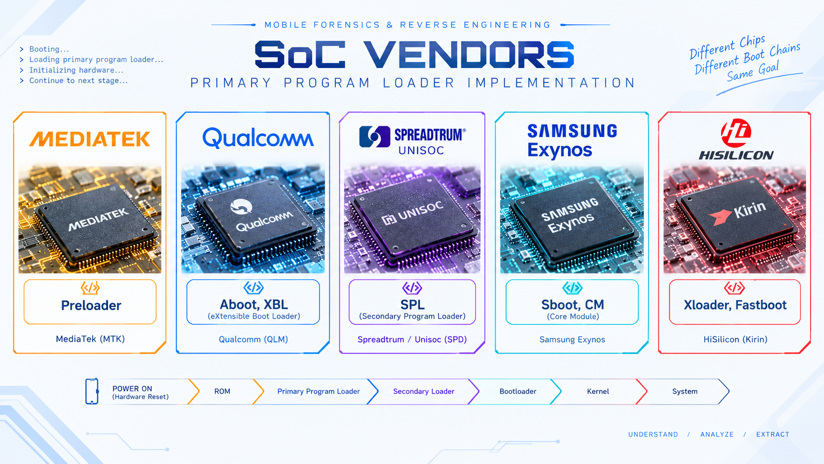
| SoC Vendor | Primary Program Loader Implementation |
|---|---|
| MediaTek (MTK) | Preloader |
| Qualcomm (QLM) | Aboot, XBL (eXtensible Boot Loader) |
| Spreadtrum / Unisoc (SPD) | SPL (Secondary Program Loader) |
| Samsung Exynos | Sboot, CM (Core Module) |
| HiSilicon (Kirin) | Xloader, Fastboot |
The firmware operates as a gatekeeper. it initializes the primary memory controller, stages volatile DRAM, verifies cryptographic signatures on verified-boot platforms, and passes execution control downstream. If any of these software components fails an integrity or presence check, the boot process halts and the device typically becomes stuck at its manufacturer logo screen
Everything above the firmware layer the kernel, the recovery image, and the Android userspace is generally referred to as software.
Mobile Storage Technologies
Non volatile memory has evolved from ROM and PROM to EPROM, EEPROM, and then flash memory. NOR flash is mainly used for running code, while NAND flash is denser, cheaper, and better for storing large amounts of data. MMC added a controller to manage NAND flash, and eMMC integrated this technology into a package designed for mobile devices. Later, UFS replaced the older MMC interface with a faster serial connection, providing higher performance and more SSD-like storage capabilities for modern smartphones.
ROM → PROM → EPROM → EEPROM → NOR → NAND → MMC/SDCARD → eMMC/EMCP → UFS/EUFS
In research i will focus on MMC and UFS cuz is the most popular mobile storage in market
EMMC vs EMCP, UFS vs EUFS
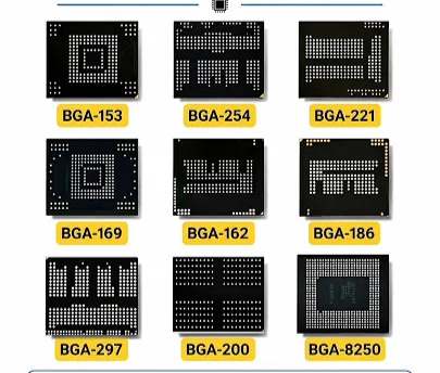
- eMMC →NAND storage with no integratedDRAM, packaged exclusively as BGA153.
- EMCP (embedded Multi-Chip Package) → eMMC combined with integrated DRAM in the same package, found in BGA221 / BGA162 / BGA254 packages.
- UFS →NAND storage with no integrated DRAM, packaged exclusively as BGA153.
- EUFS → UFS combined with integrated DRAM, found in BGA254 / BGA297 packages.
eMMC Architecture
eMMC uses a parallel data bus, and its performance improved with newer versions. eMMC 4.5 supports up to 200 MB/s, while eMMC 5.0 and 5.1 can reach up to 400 MB/s. eMMC 5.1 also introduced Command Queuing (CQ), which improves performance when handling multiple read and write operations
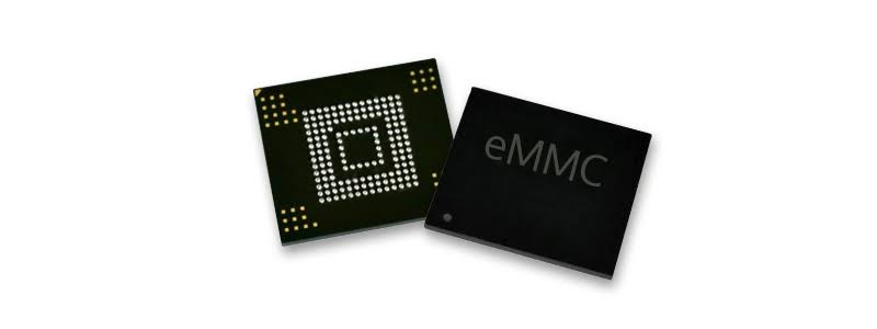
eMMC packages contain an integrated controller that abstracts the underlying flash into distinct hardware level partitions
| Hardware Block Alias | Standard JEDEC Partition | Technical Forensic Function |
|---|---|---|
| ROM1 | User Data Area | Primary storage; contains the partition index (GPT) and all OS/user volumes. |
| ROM2 | Boot Partition 1 (BOOT1) | Dedicated non-volatile boot mirror; holds primary bootloader images. |
| ROM3 | Boot Partition 2 (BOOT2) | Secondary boot mirror for redundancy and fallback. |
Vendor-Specific Boot Partition Routing
In standard embedded designs, the host SoC directs its primary boot fetch to the dedicated hardware boot partitions (BOOT1 or BOOT2)
- IN MediaTek, Exynos, and Kirin : Platforms default to reading boot stages from the physical
BOOT1/BOOT2partitions.
- IN Qualcomm : Qualcomm application processors deviate from this convention by fetching primary boot routines directly from the User Data Area (ROM1). Misidentifyingthis behavior during physical ISP extraction will lead an examiner to mischaracterize a device's boot.
Pinouts
eMMC (legacy MMC-derived parallel bus):CMD (command line), CLK (clock), DAT0–DAT7 (up to 8 parallel data lines, depending on bus width configuration ), VCC (core supply), VCCQ (I/O supply).
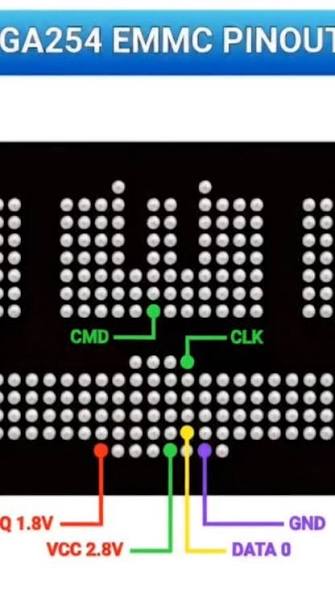
UFS Architecture
UFS uses a newer full-duplex serial interface instead of the older parallel MMC bus.
It uses M-PHY and UniPro technologies with SCSI-based commands, providing much higher performance. UFS speeds increased from about 1.2–2.9 Gbps in UFS 1.x to 23.2 Gbps per lane in UFS 4.x. However, these are theoretical interface speeds.
The actual performance is lower because it depends on the NAND flash, controller, number of memory channels, temperature, and caching.
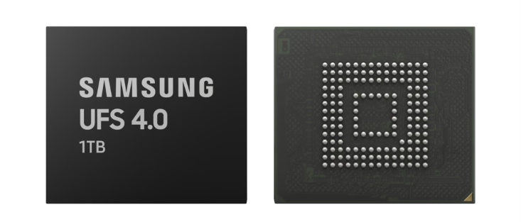
| UFS Version | Physical Link Gear | Approx. Speed per Lane |
|---|---|---|
| UFS 1.x | HS-G1 / HS-G2 | 1.2–2.9 Gbps |
| UFS 2.0 / 2.1 / 2.2 | HS-G3 | 5.8 Gbps |
| UFS 3.0 / 3.1 | HS-G4 | 11.6 Gbps |
| UFS 4.0 / 4.1 | HS-G5 | 23.2 Gbps (~46.4 Gbps across dual lanes) |
UFS replaces physical hardware partitions with SCSI Logical Units (LUNs). Dedicated boot LUNs typically designated Boot LUN A and Boot LUN B hold redundant stages of the initial bootloader.
SoC LUN Allocation
UFS organizes storage using Logical Units (LUNs) instead of the traditional physical partitions used by eMMC. Dedicated boot LUNs, usually Boot A and Boot B, store separate copies of the bootloader to provide redundancy. The exact LUN used for each boot stage depends on the SoC manufacturer and its Boot ROM configuration
| SoC Vendor | eMMC Boot Source | UFS Boot Source |
|---|---|---|
| Samsung Exynos | BOOT1 / BOOT2 | Boot A (LUN1) / Boot B (LUN2) |
| MediaTek | BOOT1 / BOOT2 | Boot A (LUN0) / Boot B (LUN1) |
| HiSilicon (Kirin) | BOOT1 / BOOT2 | Boot A (LUN0, Xloader) / Boot B (LUN1, Fastboot) |
| Qualcomm | User Area (ROM1) | Boot A (LUN1: Primary GPT, XBL), Boot B (LUN2: Secondary GPT/Backup) |
UFS communications operate across two M-PHY physical signaling profiles:
- PWM-Gear (Pulse Width Modulation): Low-speed, low-power modes (PWM-G1 through PWM-G7) with throughputs ranging from 3 to 9 Mbps. PWM is used during link initialization, power-state negotiations, and recovery modes.
- HS-Gear (High Speed): Multi-gigabit modes (HS-G1 through HS-G5) designed for system execution, app loading, and active read/write operations.
During forensic hardware diagnostics, forcing a UFS memory link back to its base PWM operating mode allows examiners to verify the electrical and signal integrity of the storage bus when higher-speed HS handshakes fail due to line noise or physical board damage
Pinouts
UFS (serial, differential, UniPro/M-PHY-based):
TX0P / TX0N (differential transmit pair, DIN0_T / DIN0_C),
RX0P / RX0N (differential receive pair, DOUT0_T / DOUT0_C),
CLK (reference clock), RESET, VCC (core supply), VCCQ1 and VCCQ2 (separate I/O supply rails, reflecting UFS's dual-voltage-domain design).
Storage Indexing & Android Volumes
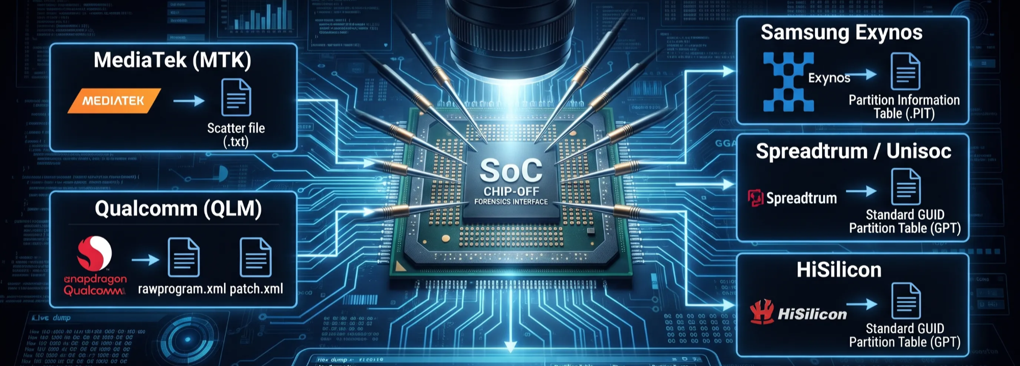
Once a storage device initializes, the host processor interprets the data block layout via a partition table located at the head of the user data address space
| SoC Manufacturer | Partition Indexing Format |
|---|---|
| MediaTek (MTK) | Scatter file (scatter.txt) |
| Qualcomm (QLM) | rawprogram.xml and patch.xml |
| Spreadtrum / Unisoc | Standard GUID Partition Table (GPT) |
| Samsung Exynos | Partition Information Table (.PIT) |
| HiSilicon | Standard GUID Partition Table (GPT) |
Structural of Android Storage Volumes
- Discrete Partition Architecture (Pre-Android 10): Independent EXT4 partitions allocated directly on flash (
/system,/vendor,/boot,/recovery,/data,/efs).
EFS holds cryptographic radio calibration data and the baseband IMEI.
- Dynamic Partitions (
superpartition, Android 10+): Consolidates runtime OS images (system,vendor,product,odm) into a single raw container partition designatedsuper.
This design improves storage allocation flexibility, but requires forensic carving tools to parse custom Device-Mapper-Linear metadata structures.
RPMB Binding Constraints

RPMB is a protected area in eMMC and UFS storage used to store important security information, such as anti-rollback counters and secure-boot data. It uses a secret authentication key and a write counter to make sure data is trusted and cannot be replayed or replaced with an older version. Unlike normal user storage, RPMB is designed to keep this security state even after a factory reset or re-flashing the device.
Mechanism
Authentication key
A 256-bit symmetric key is programmed into the storage device once, at manufacturing time, in a controlled/secure environment.
Write authentication
Every RPMB write must include a Message Authentication Code (MAC), typically HMAC-SHA-256, computed over the write frame and the shared authentication key. Reads are unauthenticated by default but return data whose authenticity can be checked the same way.
Replay protection
A monotonically increasing write counter, maintained by the storage device itself, is included in the MAC computation for every write.
Because the counter always increases, a captured (write request, MAC) pair cannot be successfully replayed later the counter value would no longer match, and the MAC would fail to verify.
JTAG acquisition is mainly used when a device cannot boot normally, USB debugging is unavailable, or the bootloader prevents other acquisition methods. It also requires the board to expose accessible JTAG/TAP test points. However, JTAG is usually not the first choice because it is more invasive, slower, and carries some risk of damaging the board. If logical, file-system, or standard physical acquisition works, those methods are generally preferred.
JTAG vs. ISP vs. Chip-Off
JTAG (Joint Test Action Group)
JTAG leverages the IEEE 1149.1 boundary scan interface originally designed for circuit integrity verification.
By soldering leads to the Test Access Port (TAP) comprising TDI (Data In), TDO (Data Out), TCK (Clock), and TMS (Mode Select) an examiner instructs the SoC's debug engine to halt execution and dump memory contents across the internal bus.
The TAP Controller is a 16-state system controlled by TCK (clock) and TMS (control). It decides whether the chip is reading, shifting, or updating data. The Instruction Register (IR) selects what operation the chip should perform, such as IDCODE, EXTEST, SAMPLE/PRELOAD, or BYPASS. After selecting an instruction, the corresponding Data Register (DR) is used to send or receive data through TDI/TDO. The Boundary-Scan Register (BSR) contains cells connected to the chip's I/O pins, allowing a tester to read or control the signals on the pins without directly accessing each pin individually.
Advantages, Limitations, Risks
JTAG forensic acquisition generally involves connecting directly to test points on the device's board using a JTAG adapter. The tool communicates with the SoC through its debug interface to access the device's memory without relying on the normal OS or bootloader. The acquired data is then saved as a raw image, immediately hashed (such as with SHA-256), and documented for chain of custody. Finally, the image is checked to make sure the expected partitions and filesystem structures are present before analysis.
limitations
JTAG has several limitations. It is not a universal way to bypass Android security and cannot automatically decrypt FBE/FDE-protected data. Some devices disable JTAG completely, while finding the correct test points can be difficult and may risk damaging the board. JTAG also only provides access to what the SoC and its current firmware state allow, so it does not guarantee a complete dump. Finally, JTAG procedures are often specific to the exact device and board revision, meaning a method that works on one version may not work on another.
ISP (In-System Programming)
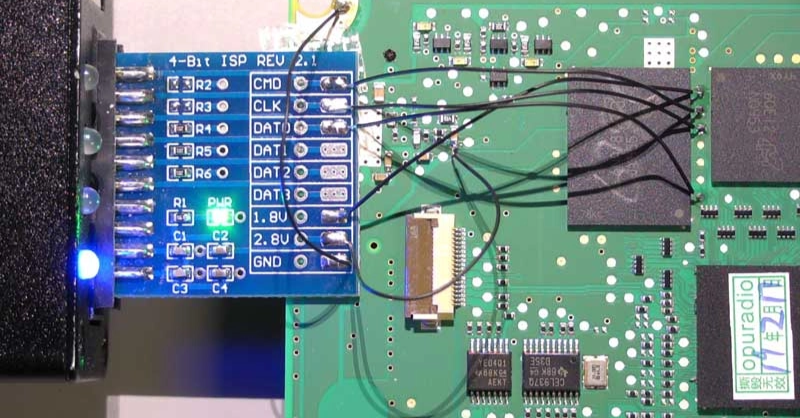
ISP refers to directly interfacing with the storage chip's native protocol (the eMMC/MMC command bus, or the UFS UniPro/M-PHY link) while the chip remains soldered on the board.
ISP extraction reads the storage directly from the motherboard without using the phone's SoC. Very thin wires are soldered to test points connected to the memory's communication lines, such as DAT0, CMD, and CLK, along with power and ground. The memory chip stays on the board, while an external programming tool communicates with it and extracts the data.
eMMC ISP vs. UFS ISP
- eMMC ISP connects to the CMD/CLK/DAT lines and issues standard eMMC bus commands directly, reading the User Data Area, Boot Partitions, and RPMB.
- UFS ISP is more difficult than eMMC ISP because UFS uses a high-speed differential serial connection instead of simple parallel data lines. The examiner must correctly handle things like clocking, reset, and communication speed (gear) negotiation. If the external tool and UFS device do not use compatible settings, the storage may not be detected at all.
Advantages, Limitations, Risks
Advantages: does not require desoldering the chip, can work on devices where JTAG test points are unavailable or fused off, generally faster to set up than chip off once test points are identified.
ISP also has some limitations. It requires accurate identification of test points, which are often undocumented, and poor soldering or too much heat can damage the board or storage chip. UFS ISP is especially complex compared with eMMC ISP.
Also, the extracted raw image may still be encrypted, and ISP does not automatically provide access to RPMB, since RPMB requires its authentication key
Chip-Off
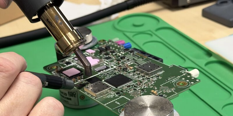
Chip-off acquisition physically desolders the NAND flash package (eMMC/UFS/EMCP/EUFS) from the PCB and reads it directly in a compatible chip reader/adapter, bypassing the SoC, bootloader, and OS entirely.
Chip-off acquisition involves removing the storage chip from the motherboard using controlled heating, then cleaning and sometimes re-balling the chip before placing it in a compatible reader or adapter. The reader then extracts the raw storage image. With eMMC, this can include the User Data Area and sometimes the Boot Partitions. For UFS, a UFS-capable reader is required because it uses the UniPro/M-PHY protocol, making UFS chip-off more specialized than eMMC.
Chip-off has several advantages. It can work even when the motherboard is severely damaged, as long as the storage chip is still intact. It also bypasses SoC-level restrictions, so things like a locked bootloader or disabled JTAG no longer matter. In addition, it can usually provide access to most or all readable NAND storage blocks, making it one of the most comprehensive physical acquisition methods.
Chip-off also has important disadvantages. It is destructive because the storage chip must be removed from the board, and the device may no longer be practical to restore. It requires specialized adapters that match the exact chip package.
The storage controller also performs wear leveling and address mapping, so the raw data must be correctly interpreted by the reader software. Finally, even a complete raw image may still contain encrypted data (FBE/FDE) that cannot be directly read without the required keys.
This section reorganizes "best case / worst case" for repair guidance.And reflects field repair industry knowledge based on a real world hardware cases
SoC-Specific Vendors
MediaTek

Best case: a storage device that is speed compatible with the target board and has a "clean" RPMB region.
Boot path: eMMC boots from Boot Partition 2/3. UFS-based MediaTek platforms boot from Boot A (LUN0) / Boot B (LUN1)
Worst case:a non clean RPMB still allows the device to boot but can produce app level failures, speed incompatible replacement storage will not function, such as the camera, may stop working.
An incorrectly configured boot path or corrupted firmware write will prevent boot.
Qualcomm

Best case: speed compatible, RPMB-clean storage
RPMB replaceability is described as chipset generation dependent:
Qualcomm chips at or below the Snapdragon 425 tier, the chipset itself can (re)generate clean RPMB keys, above that tier (450 and up), RPMB keys must be extracted from the original chip (if accessible) using specialized hardware ( "F64 box," a repair industry chip-reader tool)
If the device uses UFS, replacing the storage may not be possible because the RPMB sector is encrypted and cannot be directly extracted or transferred.
Samsung Exynos
Best case: speed compatible, RPMB clean storage.
Worst case: a non clean RPMB still boots the device but, on eMMC platforms, prevents unlocking the bootloader, on UFS platforms, the camera subsystem is reported to fail.
Speed-incompatible replacement storage (installing an older-generation eMMC/UFS chip from a legacy device) will not function.
HiSilicon (Kirin)

Best case: speed compatible, RPMB-clean storage.
RPMB replaceability is again described as chipset generation dependent:
Kirin 659 and below reportedly allow normal eMMC replacement because the chip can generate clean RPMB keys itself.
Kirin 710 and above reportedly cannot, requiring RPMB key extraction from the original chip via a specialized reader ("F64 box") if available.
UFS-based HiSilicon devices are described as not supporting RPMB replacement at all due to RPMB sector encryption.
U think this is the end bruhhh no i have a surprised
Practical Case Study with HONOR X7d
I didn’t want to keep this research purely theoretical, so I decided to take it a step further and turn one of the techniques I studied into a real world practical experiment.
In mobile forensics, we often study acquisition methods through technical papers, training materials, and demonstrations. We learn about JTAG, ISP, and Chip-Off, understand how they work in theory, and explore the tools used to access device memory.
But understanding a technique on paper is one thing. Watching it happen on a real device is something entirely different.
I wanted to move beyond the theoretical side of mobile forensics and see what happens when these techniques meet real hardware, a real motherboard, tiny connection points, specialized equipment.
So, I decided to visit a mobile repair shop and turn the research into a practical experience
The main objectives were to:
- Understand the physical structure of the target device and identify the relevant hardware components.
- Explore connection using ISP acquisition approach
- Observe how specialized equipment is connected to a smartphone motherboard.
- Understand the technical and evidential limitations that remain after a memory read attempt.
so, let’s go
Before attempting any hardware level acquisition, the first step is to understand the target device
its processor, RAM, internal storage, and the way these components interact
For this research, the target was an HONOR X7d 4G, identified during the practical session as model LGN-LX3.

Just open the http://gsmarena.com/ then search with mobile model
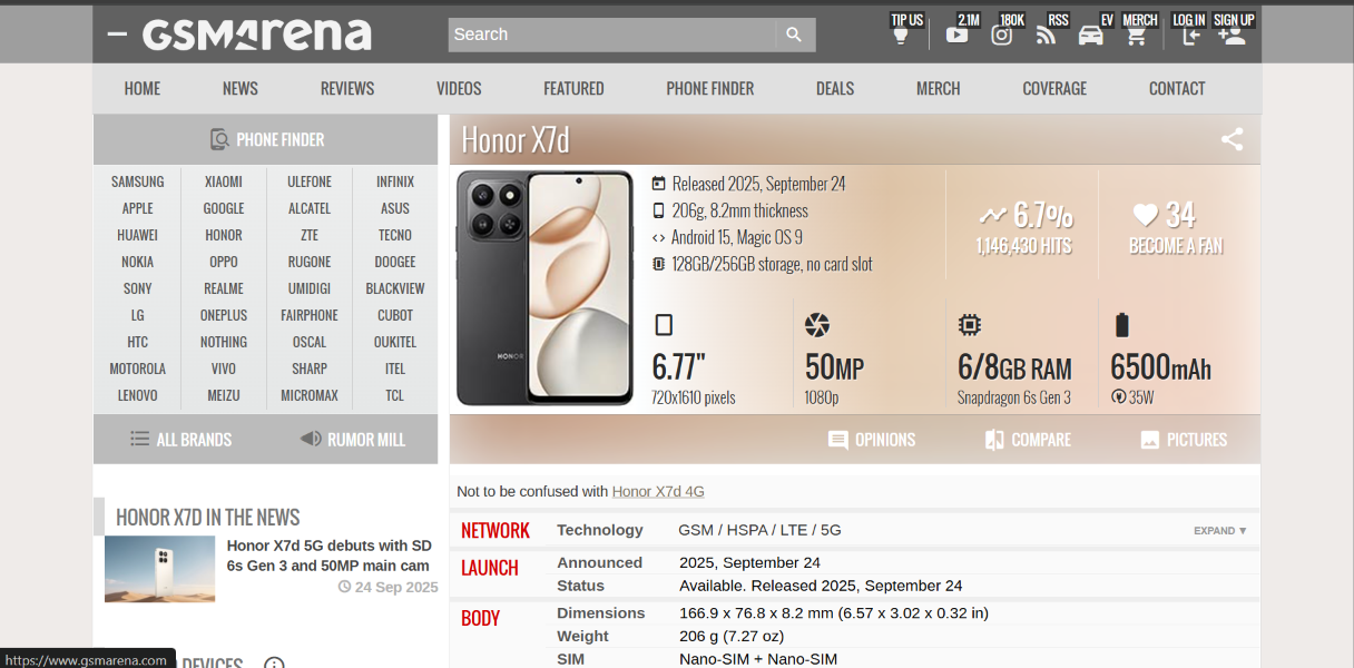
Main part in this research

The HONOR X7d 4G is an Android smartphone built around a Qualcomm Snapdragon platform Public specification listings associate this variant with the Snapdragon 685 processor, LPDDR4X RAM, and UFS 2.2 internal storage.
In this mobile the technician decide to using ISP by Flash64 Box. In this guide, we will also guide you on how to connect the ISP pinout to Flash64 Box
Also by using this box, you can easily restore the stock ROM, bypass FRP lock, remove MDM Lock, repair a Dead Boot, or reset user data on your device
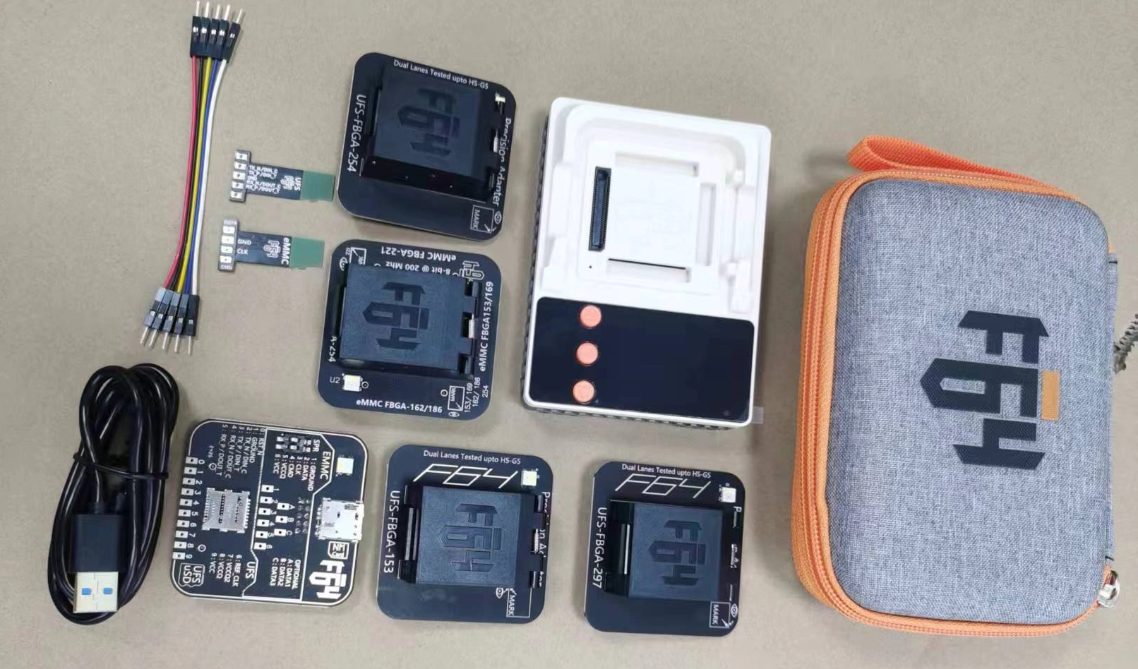
The F64 box is a translator it sits between your laptop and the phone's storage chip, and it talks to the chip through a few thin wires. Only six things matter on those wires: power, ground, a clock, a command line and a data line.
So here we go, The first step was to open the back of the phone
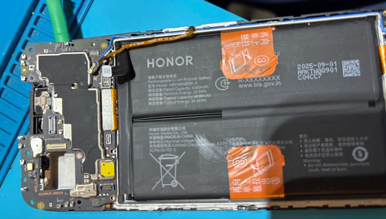
During this stage, care was required to avoid unnecessary pressure on the display, frame, and internal components, as physical damage could affect the device condition.
After opening the mobile, Disconnecting the battery is an important preparation step during many hardware level procedures because it reduces the risk of accidental electrical shorts while working around exposed connectors and motherboard components
Then the technician decide to take the motherboard completely out of the housing to drill in processor under the microscope
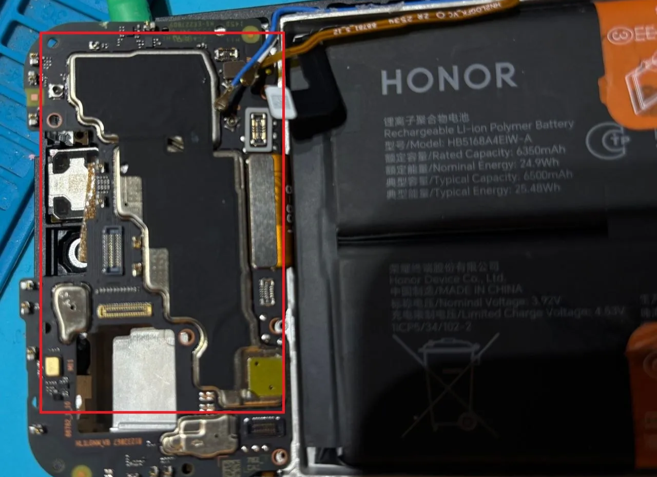
The reason it’s valuable is the ISP pinout. This process needs to drill into the CPU layers to access data lines, as the required lines are visible on the PCB layer
Then the technician take the motherboard under the microscope and scrape off the protective coating or remove a small part of the metal shield or EMI shielding to reach them.
IF you remember we talked above about UFS communication, and this in the lines in the motherboard after drilling , should connect the pins out of the F64box on it
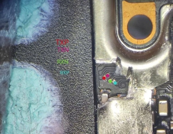
Pinouts
RST:Hardware reset pin
TX0_P: Transmit positive signal
TX0_N:Transmit negative signal
RX0_P: Receive positive signal
RX0_N: Receive negative signal
GND : Connect to any ground point
VCC: Main power supply (typically 2.5V or 3.3V)
VCCQ2: I/O power supply (typically 1.8V)
Each data direction uses a differential pair consisting of two signals, The two pairs serve different directions
- TX pair: Transmits data from one interface endpoint to the other.
- RX pair: Receives data from the opposite direction
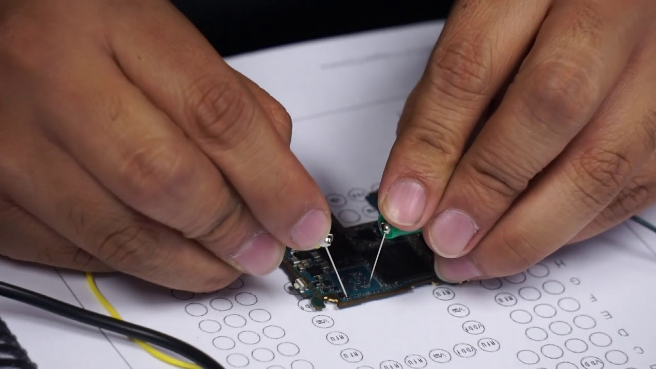
Then he started taking the 0.1 mm jumper out of the F64 box to connect it and taped the jumper down to stay in place and not move, which could otherwise damage the lines
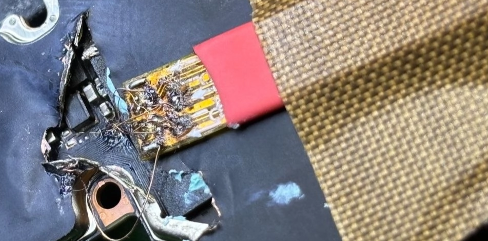
Connect jumper wires to Rst, Txop, Txon, Rxop, and Rxon points with care using solder.
then doublecheck each wire using a multimeter to ensure there are no shorts
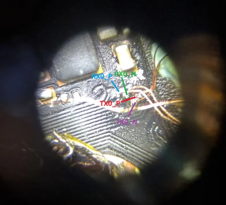
This is a close up image under a microscope
After identifying the intended connection points on the PCB, fine wires were soldered to the selected points under a microscope. These wires were then connected to the F64 box using the appropriate connection interface
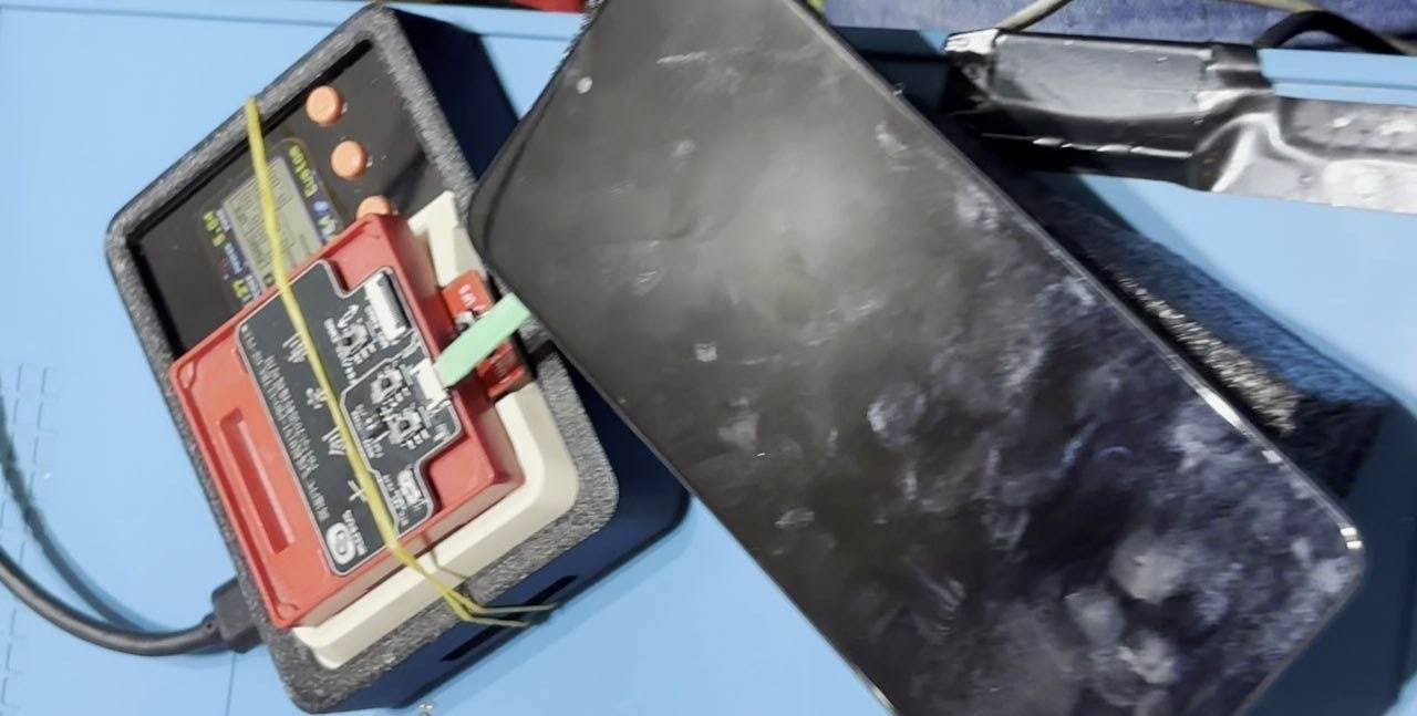
As U see the mobile connected directly with box
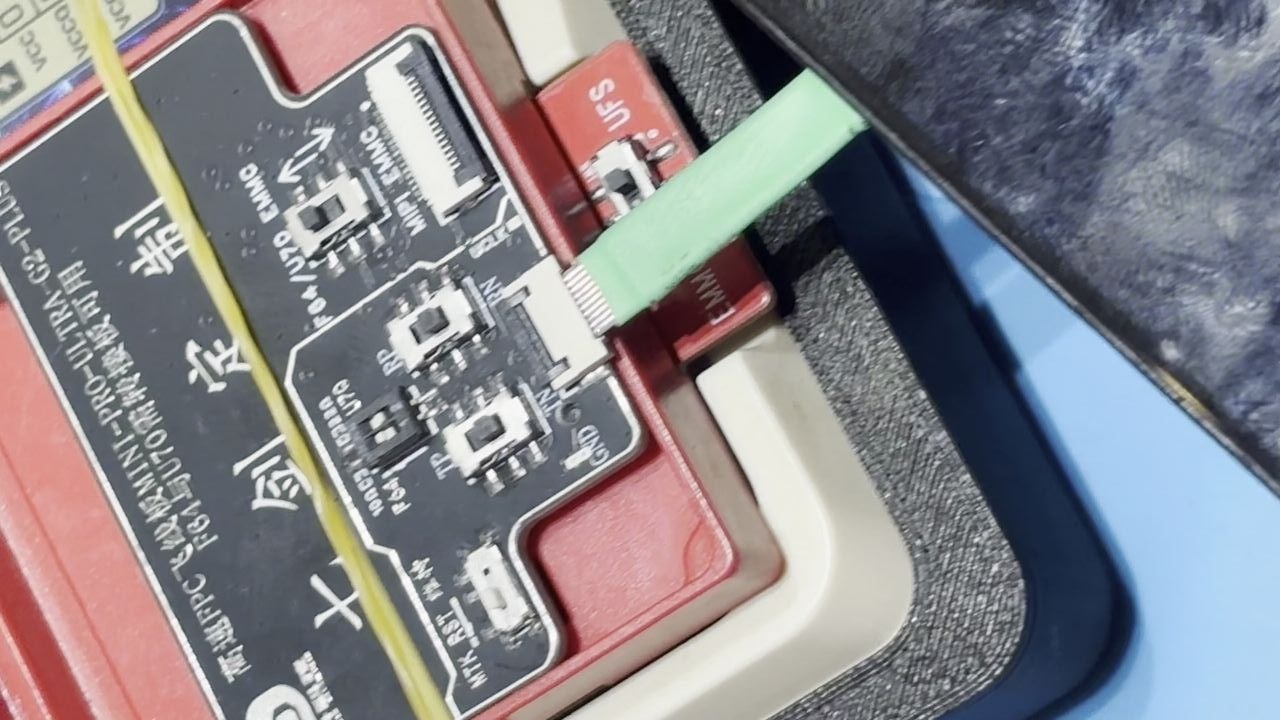
Once the hardware connections were established, the F64 box was connected to its associated software application
That’s great, we have finished 90% of the mission, the next step is connect the box between the software of the box and chip.
Once the connection is established and the all connection is right (btw this step is so hard, takes a lot of time (^o^) to Fine tuning it)
So, let’s goo
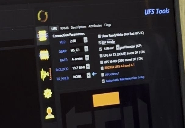
After connecting the hardware setup to the associated software, the UFS Tools interface was examined to review the available configuration parameters. The interface displays several parameters related to UFS communication, including the VCC voltage, gear, rate, and reference clock (R.CLOCK)
The UFS communication parameters must be selected according to the target storage chip specification, including its manufacturer, model, and supported UFS version
After set the configuration, then connect, finnnalllyy the chip connected successfully
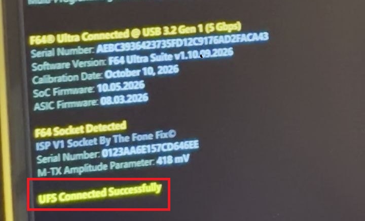
After that all device information related to phone will appear
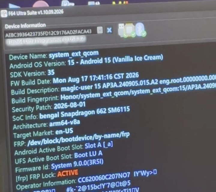
bruhhhh, we gottttt it
The F64 Ultra Suite interface displayed a list of identified storage partitions. These included partitions such as , userdata, vendor, misc, metadata, keystore, and among others. The interface also displayed partition related information, including reported sizes and filesystem labels where available.
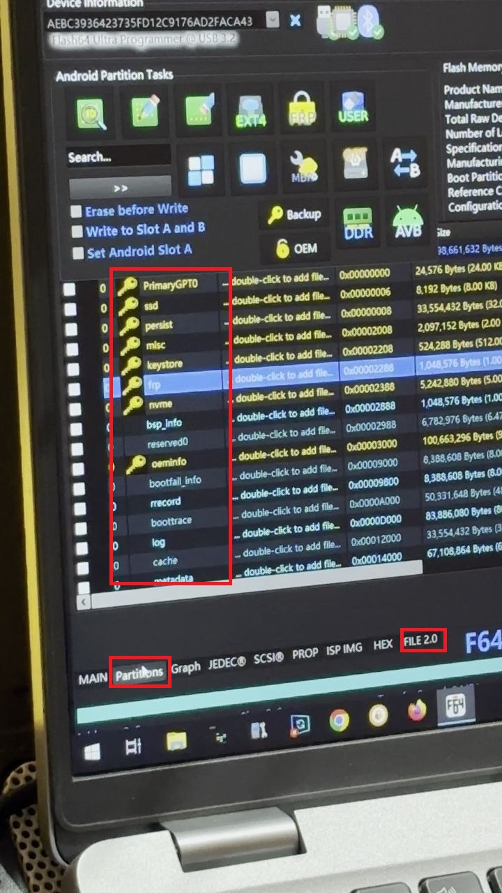
User data, including application data and other user related information also showed a Linux EXT4 filesystem label for this partition.
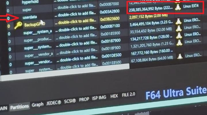
At this stage, an important limitation became apparent
Android devices comonly use file-based encryption, with encryption keys and access conditions tied to the device's security architecture. Consequently, even when a forensic tool can read storage sectors or identify the userdata partition, the underlying content may remain encrypted. Without the appropriate keys and the necessary conditions for decryption, the acquired bytes may not reveal readable application files, messages, photographs, or other user content
This highlights one of the major challenges in hardware based mobile forensics. And the experiment demonstrated both the capabilities and the limitations of acquisition
Acknowledgements
This study would not have been possible without Eng. Rezk, the repair technician who opened his workshop and shared his hands-on experience. He helped me mill into the processor stack, solder the wired pins and connect the device to the F64 box. What started as a question in my head became a real, practical experiment because of his time, skill and patience. Thank you, Eng. Rezk. 🙏